Understand the function and work of a T.con module T.con board or T.con module or sometimes called Control board;
Is a small pcb that is separated from the LCD glass panel, and connected using flatwire to the glass panel
But there are also those who stick together and form one unit with a glass panel. Sometimes it can be below or
sometimes there is also a section at the top of the glass panel.
Although rarely found; there is also a T.con circuit which becomes a unity with the mainboard. As far as I know,
only Panasonic sometimes uses it like this
The main functions of the T.con module are:
Changing RGB image data and horizontal and vertical synchronization signals from the coded motherboard to the
form of “LVDS analog signal” to “RGB digital signal” which is suitable for feeding to the glass panel according to the
panel resolution used.
Generating various “Digital control” or “Scan-driver” signal pulses; to control Gate-driver and Source-driver so that
images can be formed on the screen.
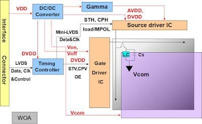
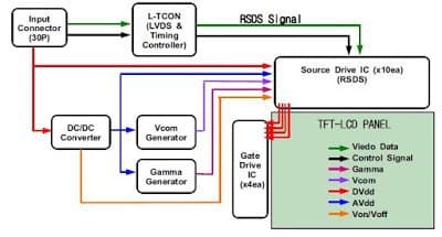
The main parts of a T.con.
Multi psu (powersuply) to provide the need for several types of voltage for Scan-drivers and for various circuits on T.con itself, for example for Gate-drivers, Source-drivers, Timing Control ICs, Gamma ICs, and other supporting digital circuits on the T module .con himself.
The V.com voltage generator is biased to the glass panel to repair the linearity of the defective characteristics of the pixel elements of the glass panel image. Sometimes this part can stand alone, but there are also sometimes become a union with Multi PSU.
IC Timing Control that functions for; (1) Changing the LVDS analog image signal to a DIGITAL RGB signal, and (2) generating various “digital timing control” signals to be fed to the Gate-driver and Source-driver.
Gamma voltage reference or Gamma Correction gray-scale voltage generator; is a set of voltage sets to improve image linearity to make it look more natural. This voltage is fed to the RGB image data signal via the Source-driver.
Level Shifter, which serves to strengthen the Gate-driver signal pulses from the IC Timing Control whose origin is only low level (approximately 0 to 3.3v) to a higher level data signal pulse, where the maximum magnitude is equal to Vgh voltage, and the minimum magnitude is equal to the voltage is negative Vgl (approximately about -10v to + 30v)
Examples of block diagram of a T.con.
From these examples it is easy to be more helpful in understanding T.con.
 Software zone